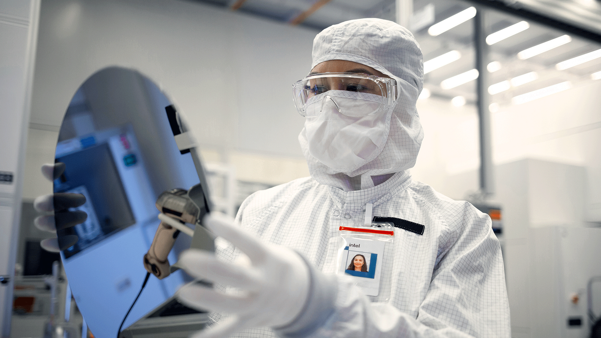
Moore's law isn't dead — it's just buried under six feet of silicon spin
Silicon wafer size is about as sensible as sizing for women's clothes.

Silicon wafer sizes aren't what you think, and those impossibly small "3nm" and "2nm" chips you keep hearing about? They're more marketing label than measurement.
The latest predictions by the Interuniversity Microelectronics Centre (IMEC), recently broken down by YouTuber TechTechPotato, presents the current timeline for TSMC's 2nm chipsets, as well as Intel Foundry's 18A and 14A process technologies, with A14 (1.4nm) chips expected in 2027 and A10 (1nm) process nodes expected in 2029. IMEC's predictions even highlight the possibility of producing 0.2mm silicon as early as 2039.
In reality, those numbers differ wildly from the physical, measurable transistors on a chip, and we may need to wait until the late 2030s before we even manage to break the 10nm barrier. Here's why.
Silicon wafers aren't as small as the 2nm size would make you think
The current 2-nanometer and 1.8nm silicon technologies in development by TSMC and Intel aren't made on wafers that are 2nm in thickness.
2nm is also not the distance between two transistors on the wafer.
Chip manufacturers tend to refer to silicon wafers based on the minimum feature size achievable on the wafer surface during fabrication. Right now, that size usually refers to the name of the process node rather than any physical feature of the chip.

In fact, since about 1997, silicon process node names have been inaccurate. Intel's 250nm process node actually had a gate length of 200nm. Intel continued this process understatement until 2011, when silicon process nodes dropped to 22nm, with an actual gate length of 26nm.
Sign up to receive The Snapshot, a free special dispatch from Laptop Mag, in your inbox.
TSMC and Samsung also adopted the "perception marketing" for silicon in 2018 with the 7nm process nodes, which were similar in gate length to Intel's 10nm silicon.
And the confusion has only continued to spiral from there.
However, if you're looking for a hard physical measurement size for the current 3-nanometer chips, they have a gate length of 16-18nm and a metal pitch of about 23nm.
So, regardless of the current 2nm and 3nm talk, we likely won't see "true" 10-nanometer silicon until IMEC's predicted sub-A2 chipset generation in 2039.
Wafer size and Moore's Law go hand-in-hand
As a quick refresher, Moore's Law is an observation in microchip design, positing that the number of transistors on an integrated circuit doubles roughly every two years. As silicon wafers get smaller, so do transistors, but eventually all things must bow to the laws of physics.
Contrary to its name, Moore's Law isn't an actual Law, but rather an observation in microchip design. Eventually, semiconductors can only get so small before circuit heat becomes a real design issue.

Nvidia's CEO, Jensen Huang, has been against the idea of continuing the Moore's Law trend largely due to the higher thermal constraints of discrete graphics cards, while CPUs like Intel's Lunar Lake chipset have more room to grow (or shrink, in this case).
But with this reminder from IMEC about the true size of silicon wafers, and the expected improvement in chip interconnect architecture and transistor technology, Moore's Law seems far from unrealistic. Whether the trend will continue past the next decade, we can't say for sure, but it looks achievable based on current projections.
That said, the potential number of transistors on those sub-A2 (10nm Lg) chipsets is staggering. The current Intel Core Ultra 9 285K has about 18 billion transistors, meaning the sub-A2 chipsets could have around 300 billion transistors in 2039.
More from Laptop Mag
- Next-gen PlayStation and Xbox consoles may have something surprising in common — but is that a good thing?
- GeForce RTX 5050 brings next-gen gaming to the masses with Blackwell laptops starting at $999
- Intel's powerful 2026 Nova Lake chip could render discrete graphics obsolete, and it was just spotted in high-performance laptops.

A former lab gremlin for Tom's Guide, Laptop Mag, Tom's Hardware, and TechRadar; Madeline has escaped the labs to join Laptop Mag as a Staff Writer. With over a decade of experience writing about tech and gaming, she may actually know a thing or two. Sometimes. When she isn't writing about the latest laptops and AI software, Madeline likes to throw herself into the ocean as a PADI scuba diving instructor and underwater photography enthusiast.

